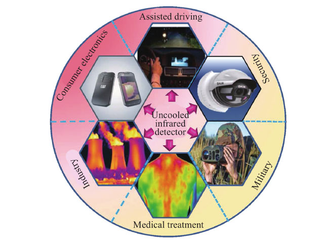
Uncooled infrared detectors are widely used in the infrared field due to their low cost, small size, and low power consumption because they do not need the cooling device and can work at room temperature. In military application field, the uncooled detector has gradually entered the application domain of previous refrigerated detector, and has been widely used in some low-cost weapon systems, even replaced the original uncooled detectors in some application fields. In the civil field, it has shown its advantages in price and ease of use, and has aroused widespread interest and attention in civil in-vehicle night vision, security monitoring and other application field. The working theory of several typical uncooled infrared detectors such as Bolometer, pyroelectric, thermopile, etc. were introduced, and the status of the main products that have been commercialized at home and abroad was enumerated, the development of pixel pitch, array specifications, performance and packaging of mainstream bolometer devices was focused, which were currently the most widely used. In addition to the bolometer, pyroelectric, SOI diode and other products that had been commercialized, some new uncooled detection technologies or new detectors were introduced in detail: such as the application of metasurfaces in enhancing absorption in certain wavebands, the research progress of new materials bolometer, new bi-material uncooled devices, graphene, quantum dots, nanowires and other photoelectric detection technologies. Finally, the future development trend of uncooled infrared detectors were predicted in the end of the review.

1 Commercial application of uncooled infrared detectors
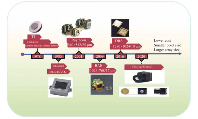
According to the working principle, the uncooled infrared detectors that have been commercialized at present can be roughly classified into the following types: pyroelectric detectors, thermopile detectors, microbolometers (hereinafter referred to as Bolometers) detectors, etc. Uncooled infrared detector technology began to develop in the 1980s, and in the early 1990s, Honeywell began to report on infrared Bolometer focal plane products [5]. The development process of uncooled infrared detectors is shown in Figure

Key Factors Affecting Bolometer Device Performance
The detection sensitivity of a device to infrared signals mainly depends on its ability to convert infrared radiation into temperature changes. For infrared radiation of the same power, the greater the temperature change of the thermosensitive material, the higher the sensitivity of the device. Therefore, in order to improve the sensitivity of the device, in addition to selecting high-quality sensitive materials, it is also necessary to minimize the loss of thermal radiation heat in the design of the device structure and packaging design to avoid heat loss caused by thermal conduction and thermal convection.
1) Bolometer sensitive material
The resistance-temperature coefficient (TCR) of sensitive materials is a key factor affecting Bolometer performance. To improve the sensitivity of the Bolometer, it is necessary to select sensitive materials with good resistance uniformity, high temperature coefficient of resistance (TCR), and low 1/f noise.
There are two routes (VOx, α-Si) in the selection of thermally sensitive thin film materials, which are different technical routes taken by the United States and France. In the 1980s, the American Honeywell Company developed the VOx Bolometer device under the auspices of the military, and then authorized several companies to produce it; while France only launched the Bolometer using α-Si in the late 1990s. Due to the early application in the United States and its huge domestic and foreign demand, the VOx material route developed in the United States currently occupies about 80% of the market share.
The TCR of VOx is generally 2%~3%/K, and the single-crystal VO2 and V2O5 prepared by special methods can reach 4%/K. From the current level of technological development, the detector using VOx thermal film material has certain advantages over α-Si in performance. VOx material has the characteristics of low noise and large TCR, and is an ideal sensitive material for preparing uncooled Bolometer arrays. :
(1) Compared with VOx, α-Si is a standard silicon process, which is easier to manufacture and has a lower cost.
(2) VOx detector can achieve higher NETD and sensitivity.
(3) The 1/f noise ratio of α-Si material is higher than VOx, the non-uniformity is poor, and the imaging quality is lower than VOx.
In the future, the two technical routes of VOx and α-Si detectors will still exist at the same time, but the market positioning will not be different. VOx is positioned in fields with higher requirements for performance and image quality, while α-Si is more suitable for civilian fields that are sensitive to price and have low performance requirements.
2) Readout circuit
The readout circuit is the core technology that limits the performance of the detector. However, since the readout circuit is matched with the detector, when reporting products, major manufacturers rarely report on the readout circuit separately, but only for the readout circuit. Some key technical indicators are explained. After knowing the indicators of the detector, the parameters of the readout circuit can be estimated. We often infer the corresponding readout circuit level based on the information disclosed by the detector [13].
Since the Bolometer is a heat-sensitive detector, it is very sensitive to small temperature changes. Early Bolometer arrays added a semiconductor cooler (TEC) on the substrate to keep the temperature stable. In recent years, with the improvement of the design level of the readout circuit, a compensation circuit has been designed to suppress the temperature drift. At present, some foreign companies have developed uncooled infrared detectors without TEC, and integrated ADC circuit on the readout circuit (ROIC), the performance is significantly improved compared with the previous detectors, and the size, power consumption and cost have reduced [14-15].
3) Package
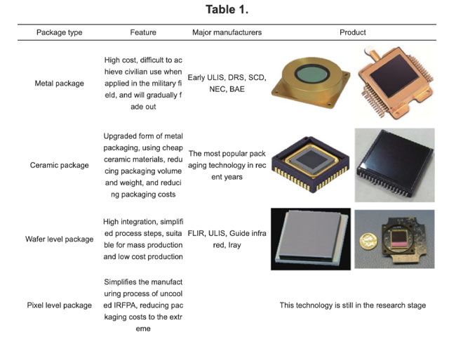
The cost and volume of uncooled detectors are the key factors limiting their applications [16]. The cost of packaging accounts for a large proportion (more than 50%) of the research and development cost of the entire detector. To reduce the cost of uncooled detectors, one of the key factors is the packaging of the device [17-19]. Packaging technologies currently in use or being developed include: metal packaging, ceramic packaging, wafer-level packaging and pixel-level packaging. The characteristics, manufacturers and typical products of several packaging technologies are shown in Table 1.

Metal shell and tube packaging is a traditional device packaging method, and its packaging structural components include metal shell (tube shell), semiconductor cooler (TEC), getter, transition substrate and infrared window. The connection between the components is mainly metal welding. High-cost components such as TEC and getter are integrated inside the package. During the packaging process, multiple process steps such as welding, adhesion, dicing and exhaust are performed. The whole process takes a long time. Long, and the number of products in each batch is limited, so the cost has been high. Products in this form of packaging are generally used in the military field, and are difficult to achieve civilian use. With the development of low-cost and high-integration packaging technology, detectors in the form of metal tube and shell packaging will gradually fade out of the thermal imaging detector market [20].
Ceramic packaging is an upgraded form of metal packaging. The packaging material uses cheap ceramic materials, which reduces the volume and weight of the packaging, and also reduces the packaging cost to a certain extent. The TEC cooler has been omitted inside the ceramic package, the tube shell used is a ceramic substrate (multi-layer wiring), and the getter is a chip or film getter, which can reduce the volume and cost of the package. After the chip is assembled, wired and other processes, the "three-in-one" sealing technology is used to complete the packaging [21]. Ceramic packaging is currently the most widely used packaging form. Domestic companies such as Iray, Dali, and Israel's SCD all use ceramic packaging for their mainstream shelf products.
Wafer-level packaging technology is currently the most cutting-edge technology in the field of device packaging, and has rapidly gained huge applications in the field of semiconductor packaging [22]. It has natural advantages in miniaturization, high integration and low cost, which is in line with the development trend of semiconductor devices, and is also the most promising new packaging form in the current uncooled infrared detector packaging technology.
Pixel-level packaging theoretically reduces the packaging cost to the greatest extent and improves the integration of packaging solutions [23]. In cell-level packing, the encapsulated object is the small cell unit in the focal plane array. In principle, the design is to deposit a cover structure on each pixel unit through microfabrication technology, and then deposit an infrared window film on each cover, so that each pixel unit is individually sealed. However, this packaging technology has not yet been introduced into China, and it is still in the technical research stage worldwide, so it will be difficult to replace chip-level packaging in the next few decades.
Both AutoNavi and Iray have launched WLP wafer-packaged VOx detectors. With the maturity of WLP packaging technology, the cost advantage ofα-Si is no longer. Iray has launched 1280×1024/12μm, 640×512/12μm wafer package FPA detectors; AutoNavi has also developed and produced 256×192/17μm and 120×92/12μm wafer package FPA detectors It is developing 400×300/12μm, 640×512/12μm and 1280×1024/12μm wafer-packaged FPA detectors.
1.1.2 Main development status at home and abroad
The main domestic manufacturers, AutoNavi Infrared, Beifang Guangwei, and Ruichuang Micronano are all in the VOx vein, and Dali Technology isα-Si. After nearly ten years of development, foreign products have no obvious advantages compared with domestic mainstream products in terms of area array size, pixel spacing and noise equivalent temperature difference. Table 2 shows the main products of domestic and foreign manufacturers that mainly produce microbolometric heat.
Table 2.
Main products of microbolometer from major manufacturer


